

Service Hotline
Products

Products

Fast Recovery Diode
The internal structure of fast recovery diode is different from ordinary PN junction diode, which belongs to PIN junction diode, i.e., the base region I is added in the middle of the P-type silicon material and N-type silicon material to form the PIN silicon wafer. Because the base region is very thin, the reverse recovery charge is very small, so the reverse recovery time of the fast recovery diode is shorter, the forward voltage drop is lower, and the reverse breakdown voltage (withstand voltage value) is higher.
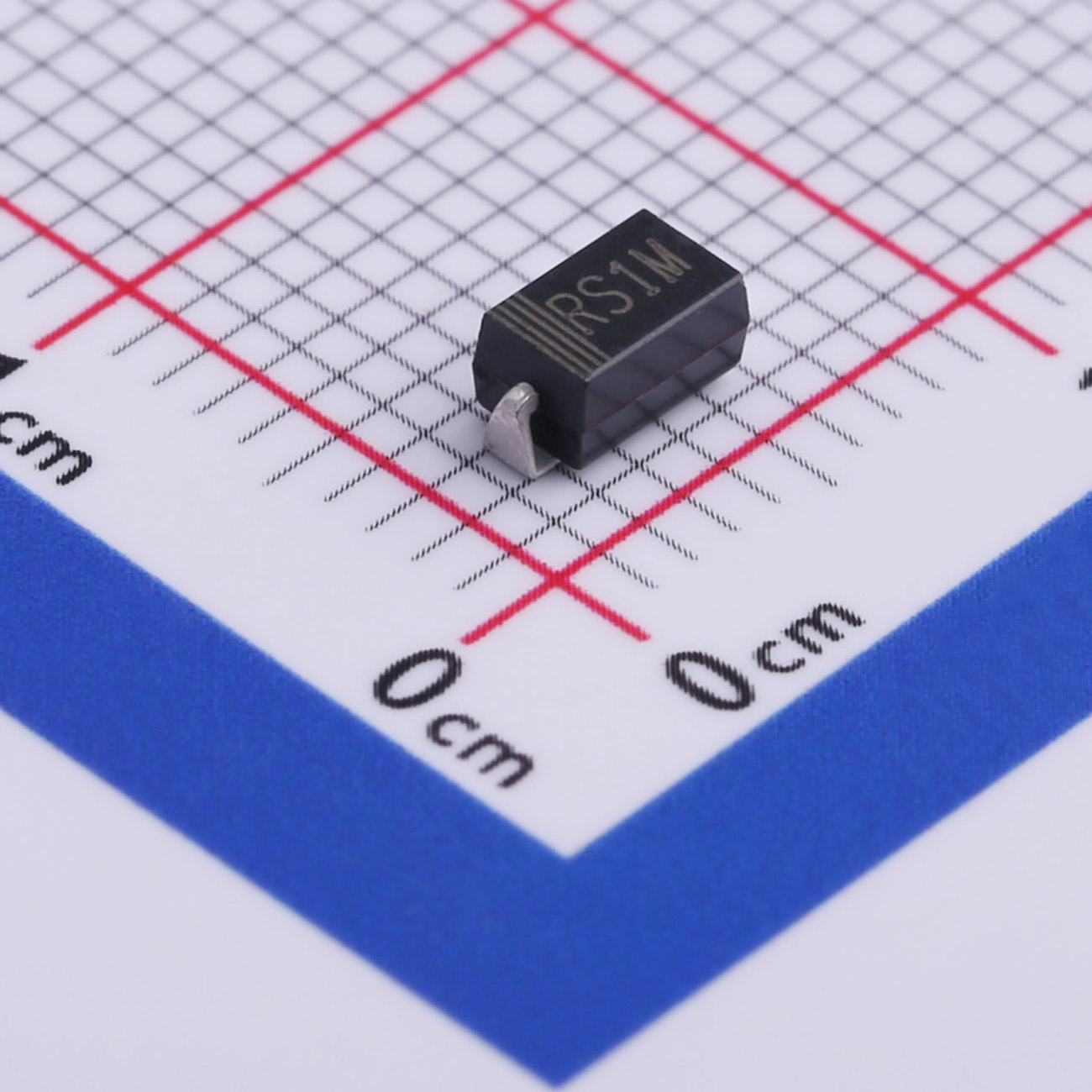
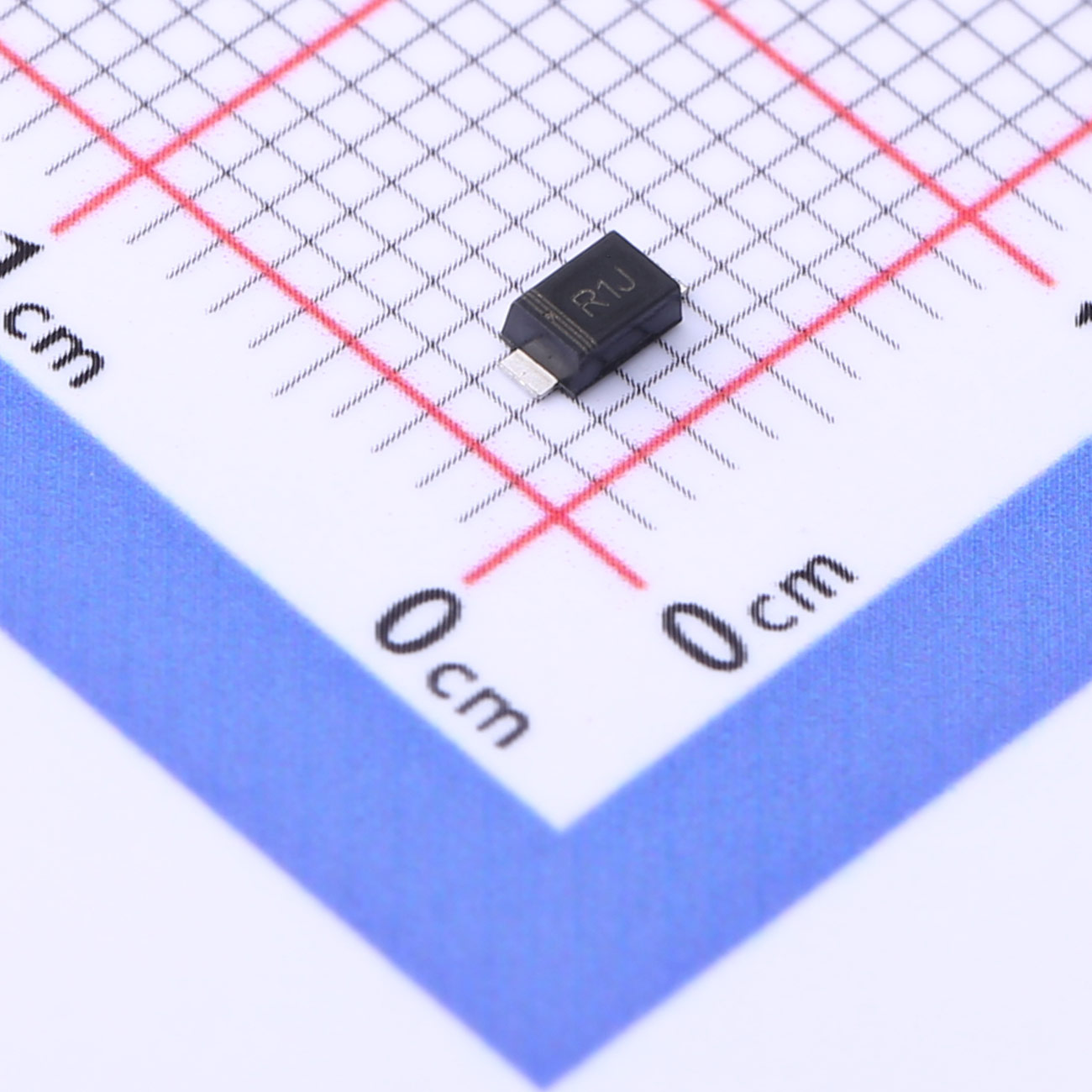
Alternative equivalent for DIODES RS1M | Slkor RS1M Surface Mount Fast Recovery Rectifier
VRRM(V):1000V
IO(A):1A
VF(V):1.3V
IR(A):5μA
trr(ns):500ns
Package:SMA
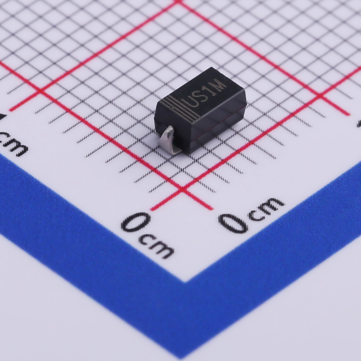
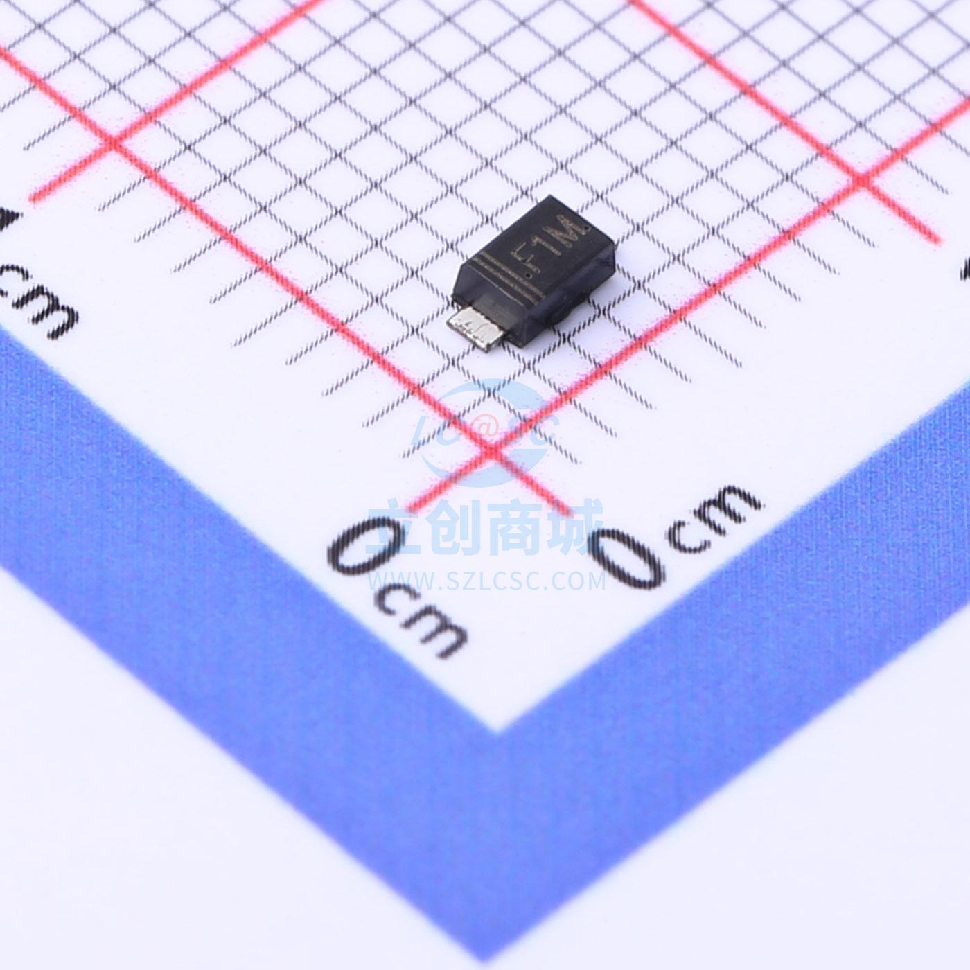
Alternative equivalent for DIODES US1M | Slkor US1M Fast Recovery Rectifier Diode
VRRM(V):1000V
IO(A):1A
VF(V):1.7V
IR(A):5μA
trr(ns):75ns
Package:SMA
Alternative equivalent for Onsemi RS1M | Slkor RS1M Surface Mount Fast Recovery Rectifier
VRRM(V):1000V
IO(A):1A
VF(V):1.3V
IR(A):5μA
trr(ns):500ns
Package:SMA
Alternative equivalent for Onsemi US1M | Slkor US1M Fast Recovery Rectifier Diode
VRRM(V):1000V
IO(A):1A
VF(V):1.7V
IR(A):5μA
trr(ns):75ns
Package:SMA
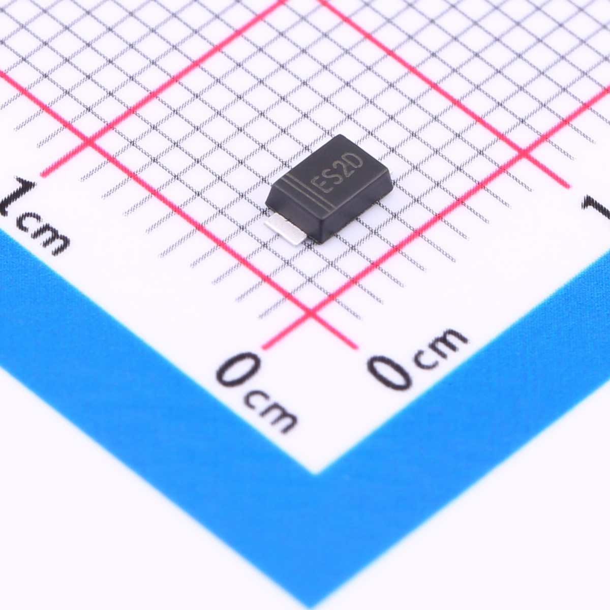
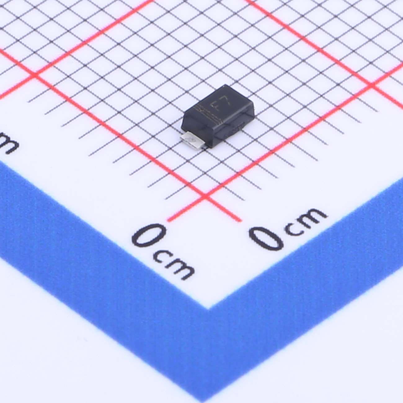
ES2DF Fast Recovery Rectifier Diode SMAF Professional Supplier
VRRM(V):200V
IO(A):2A
VF(V):1V
IR(A):5μA
trr(ns):35ns
Package:SMAF
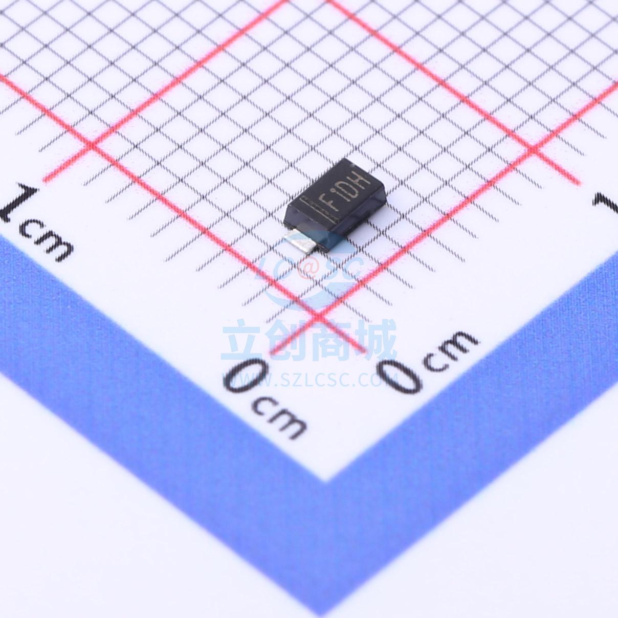
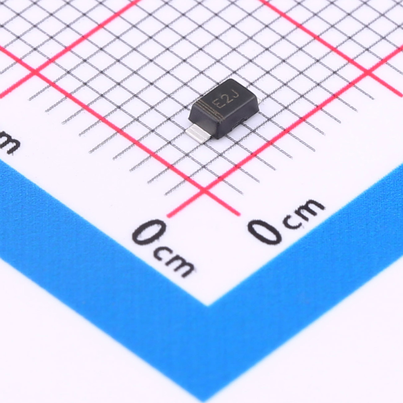
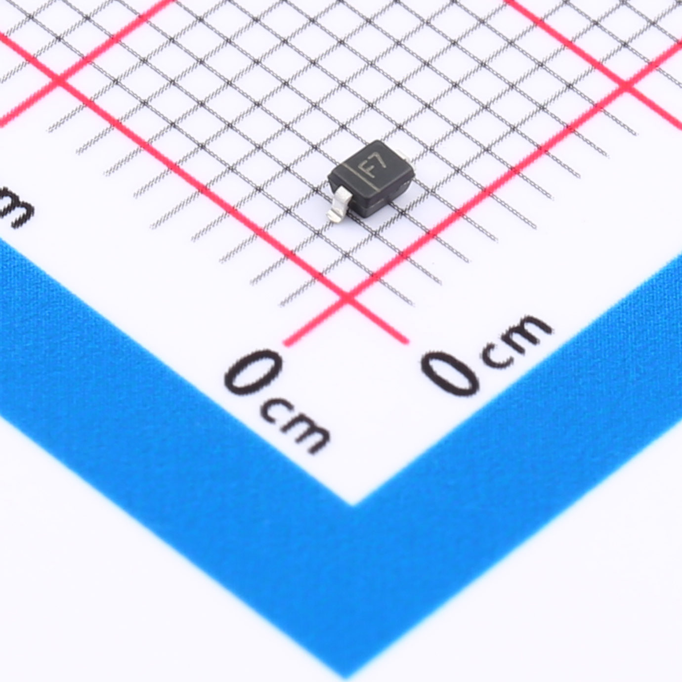
High Reliability F1D Ultra Fast Recovery Diode SOD-123FL
VRRM(V):200V
IO(A):1A
VF(V):1.3V
IR(A):5.0mA
trr(ns):150ns
Package:SOD-123FL
High Reliability F1J Ultra Fast Recovery Diode SOD-123FL
VRRM(V):600V
IO(A):1.0A
VF(V):1.3V
IR(A):5.0mA
trr(ns):250ns
Package:SOD-123FL
High Reliability F1M Ultra Fast Recovery Diode SOD-123FL
VRRM(V):1000V
IO(A):1.0A
VF(V):1.3V
IR(A):5.0mA
trr(ns):500ns
Package:SOD-123FL
High Reliability FR107 Ultra Fast Recovery Diode SOD-123FL
VRRM(V):1000V
IO(A):1A
VF(V):1.3V
IR(A):5μA
trr(ns):500ns
Package:SOD-123FL
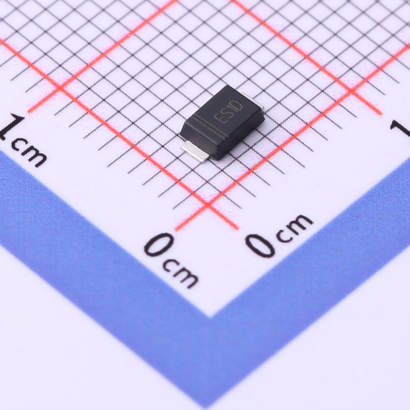
Professional Supplier ES1DF Fast Recovery Rectifier Diode SMAF
VRRM(V):200V
IO(A):1A
VF(V):1V
IR(A):5μA
trr(ns):35ns
Package:SMAF
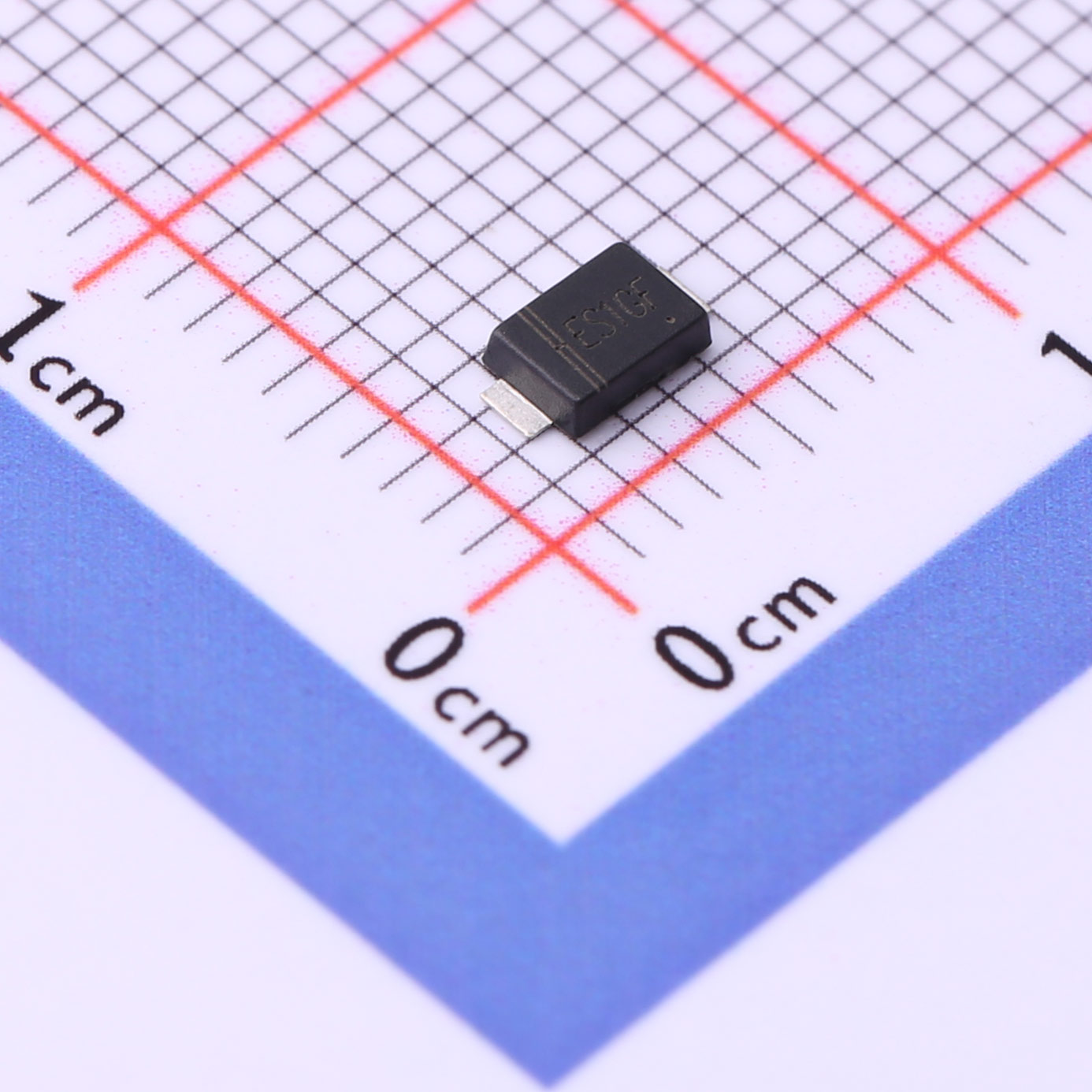
Professional Supplier ES1GF Fast Recovery Rectifier Diode SMAF
VRRM(V):400V
IO(A):1A
VF(V):1.25V
IR(A):5μA
trr(ns):35ns
Package:SMAF
Professional Supplier ES1JF Fast Recovery Rectifier Diode SMAF
VRRM(V):600V
IO(A):1A
VF(V):1.68V
IR(A):5μA
trr(ns):35ns
Package:SMAF
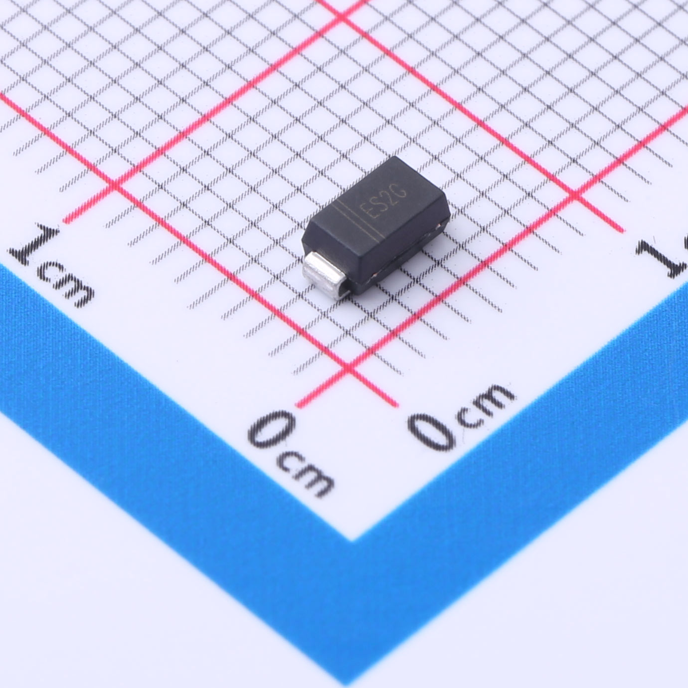
Professional Supplier ES2G Fast Recovery Rectifier Diode SMC
VRRM(V):400V
IO(A):2A
VF(V):1.25V
IR(A):5uA
trr(ns):35ns
Package:SMA
Professional Supplier ES2GF Fast Recovery Rectifier Diode SMAF
VRRM(V):400V
IO(A):1A
VF(V):1.25V
IR(A):5μA
trr(ns):35ns
Package:SMAF
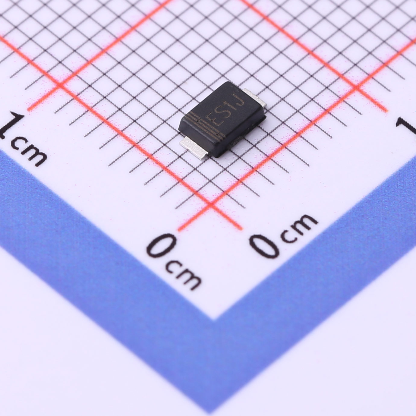
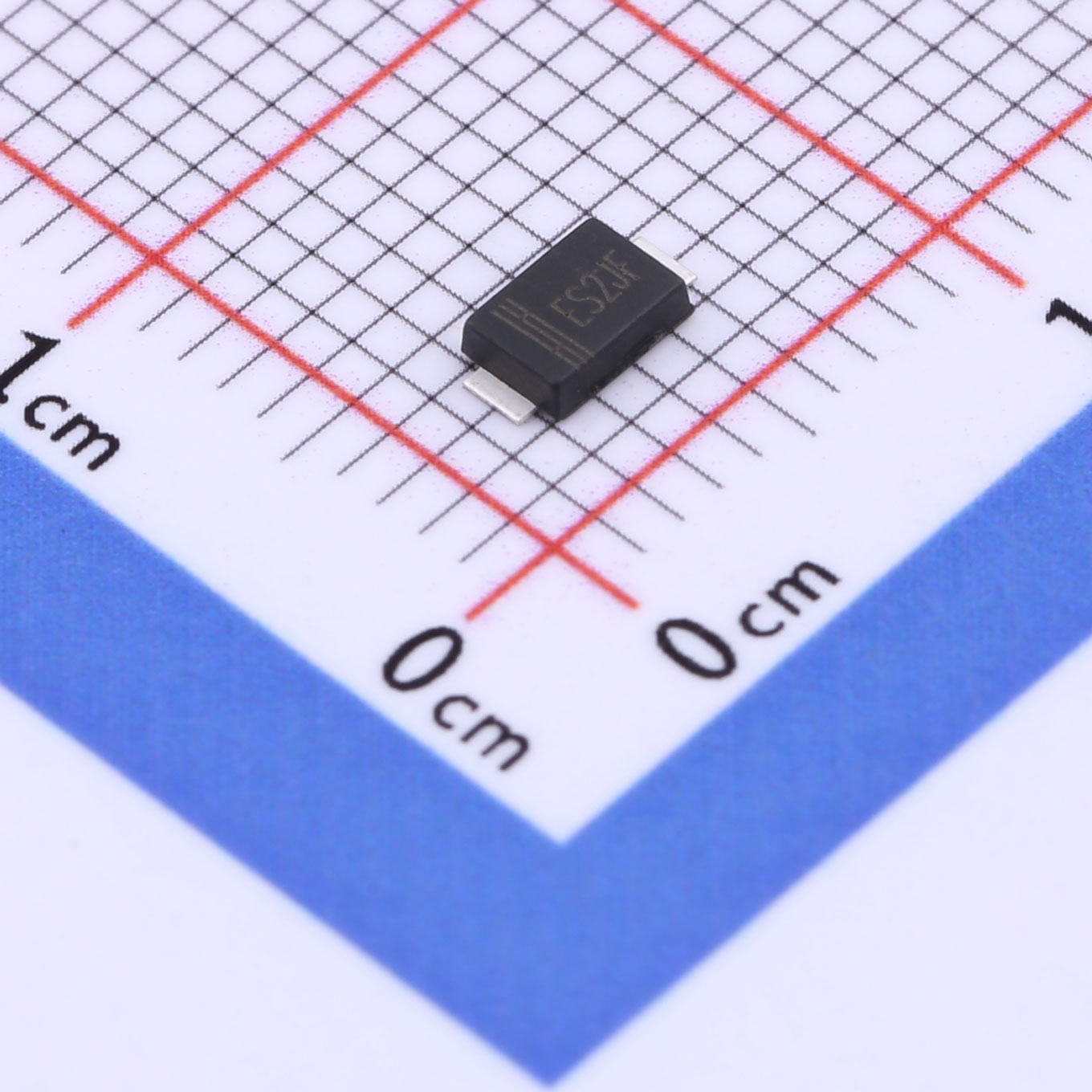
Professional Supplier ES2JF Fast Recovery Rectifier Diode SMAF
VRRM(V):600V
IO(A):1A
VF(V):1.68V
IR(A):5μA
trr(ns):35ns
Package:SMAF
Professional Supplier ES2JW Fast Recovery Rectifier Diode SOD-123FL
VRRM(V):600V
IO(A):2A
VF(V):1.7V
IR(A):5μA
trr(ns):35ns
Package:SOD-123FL
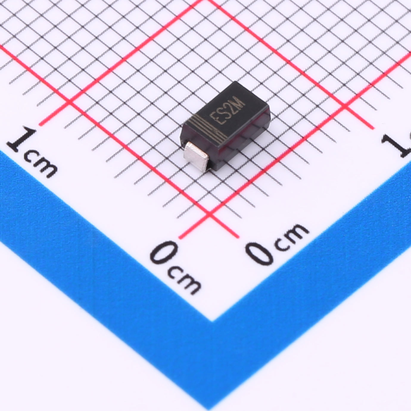
Professional Supplier ES2M Fast Recovery Rectifier Diode SMA
VRRM(V):1000V
IO(A):2A
VF(V):1.7V
IR(A):5μA
trr(ns):75ns
Package:SMA
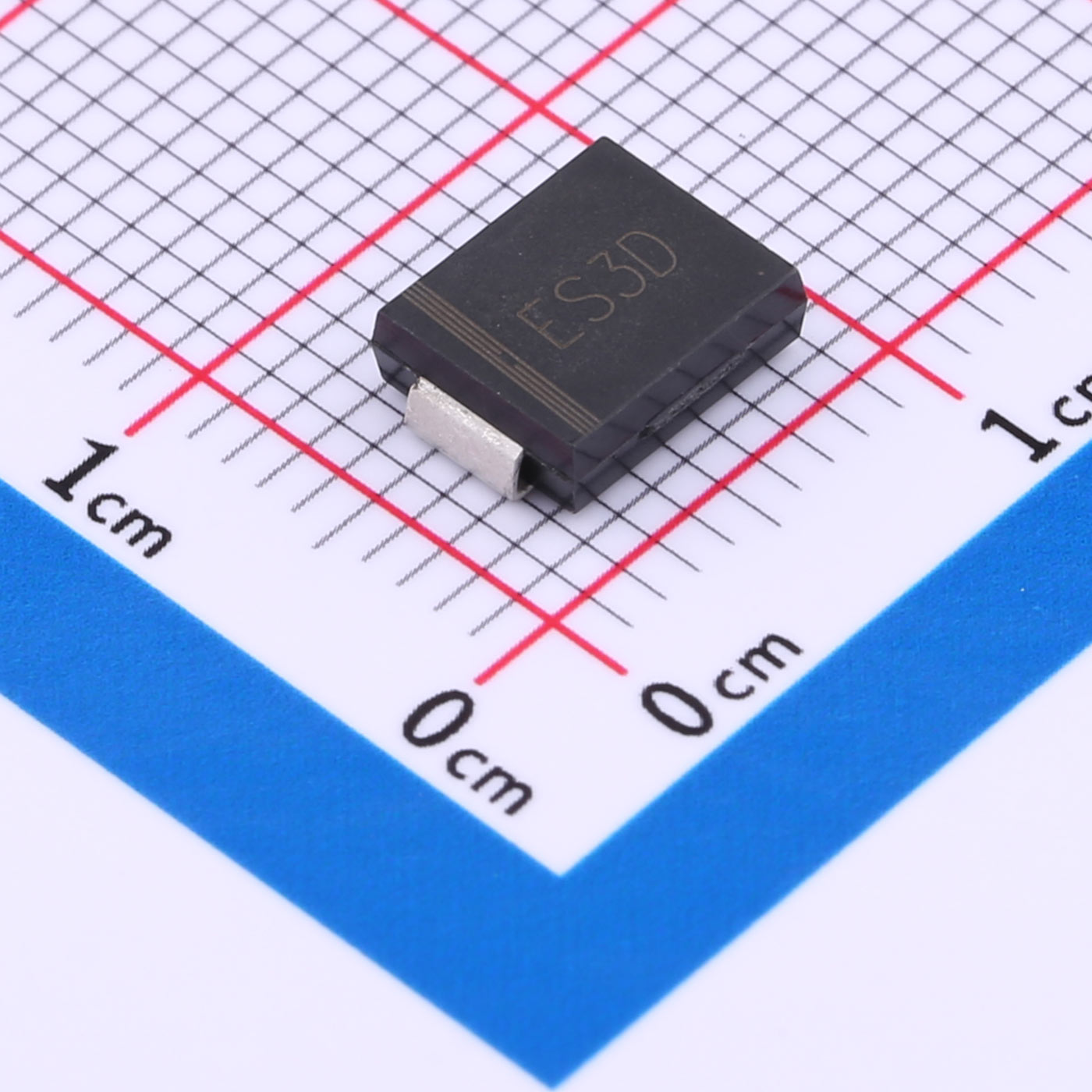
Professional Supplier ES3DC Fast Recovery Rectifier Diode SMC
VRRM(V):200V
IO(A):3A
VF(V):1.25V
IR(A):5μA
trr(ns):35ns
Package:SMC
Professional Supplier FR107WS Fast Recovery Rectifier Diode SOD-323
VRRM(V):1000V
IO(A):1A
VF(V):1.3V
IR(A):5μA
trr(ns):500ns
Package:SOD-323
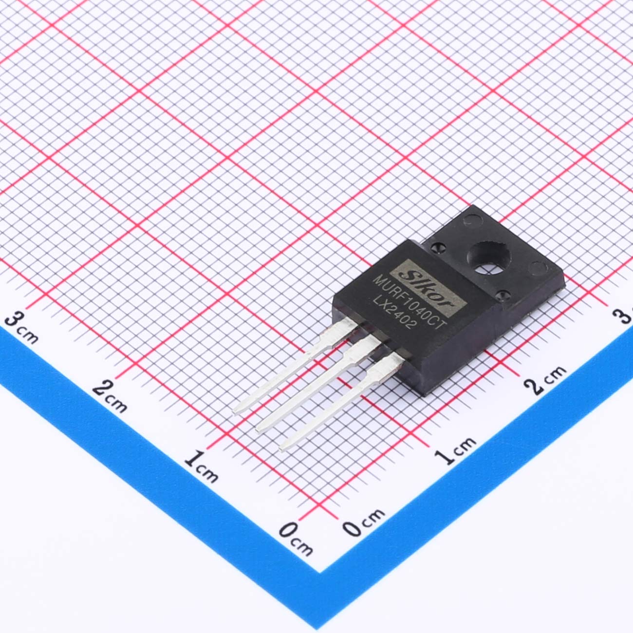
Professional Supplier MURF1040CT Fast Recovery Rectifier Diode TO-220F
VRRM(V):400V
IO(A):5A
VF(V):0.92V
IR(A):0.01μA
trr(ns):30ns
Package:TO-220F
| 1000V | 1A | 1.3V | 5μA | 500ns | SMA | |
| 1000V | 1A | 1.7V | 5μA | 75ns | SMA | |
| 1000V | 1A | 1.3V | 5μA | 500ns | SMA | |
| 1000V | 1A | 1.7V | 5μA | 75ns | SMA | |
| 200V | 2A | 1V | 5μA | 35ns | SMAF | |
| 200V | 1A | 1.3V | 5.0mA | 150ns | SOD-123FL | |
| 600V | 1.0A | 1.3V | 5.0mA | 250ns | SOD-123FL | |
| 1000V | 1.0A | 1.3V | 5.0mA | 500ns | SOD-123FL | |
| 1000V | 1A | 1.3V | 5μA | 500ns | SOD-123FL | |
| 200V | 1A | 1V | 5μA | 35ns | SMAF | |
| 400V | 1A | 1.25V | 5μA | 35ns | SMAF | |
| 600V | 1A | 1.68V | 5μA | 35ns | SMAF | |
| 400V | 2A | 1.25V | 5uA | 35ns | SMA | |
| 400V | 1A | 1.25V | 5μA | 35ns | SMAF | |
| 600V | 1A | 1.68V | 5μA | 35ns | SMAF | |
| 600V | 2A | 1.7V | 5μA | 35ns | SOD-123FL | |
| 1000V | 2A | 1.7V | 5μA | 75ns | SMA | |
| 200V | 3A | 1.25V | 5μA | 35ns | SMC | |
| 1000V | 1A | 1.3V | 5μA | 500ns | SOD-323 | |
| 400V | 5A | 0.92V | 0.01μA | 30ns | TO-220F |

Shenzhen SLKOR Micro Semicon Co., Ltd.
SLKOR's product lines include discrete devices, etc., diodes, transistors, power devices; and integrated circuit chips, etc., linear regulators, DC/ DC chips, interface chips, Hall sensors, ADCs, and BMS... We have years of accumulated technology on dedicated semiconductor.


 粤公网安备44030002007346号